|
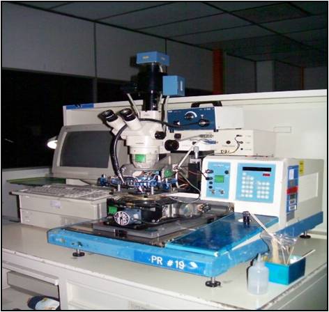
Auto Die Mounting
|
|
Purpose:
To mount the wafer into a mylar tape and attach to metal frame.
Equipment Type:
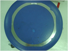
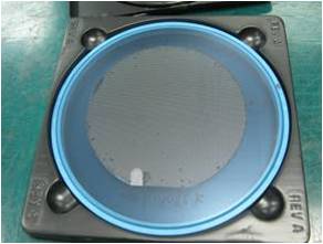
- K&S ring
- Disco ring
- Wafer ranges from 2”, 3”, 4”, 5”, 6” & 8”
Manufacturing Capabilities:
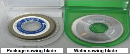
- PCB Sawing
- Molded Package Sawing
- Ceramic Substrate Sawing
- PZT wafer sawing
- SiC , GaAs Wafer Sawing
- Electrical test on Vf, Vr and LOP
- 30x -100x wafer inspection
- Provide 100% Die Visual services
|
Die Sawing and Mounting
|
Purpose:
To singulate units from a wafer or substrate form.
Equipment Type:
Disco / TSK (Straight & Bevel Cut: Single/Dual Head Spindle / Laser Saw)
Manufacturing Capabilities:
- K&S ring and Disco ring
- Wafer Thickness from 0.05mm to 0.32mm
- Saw street: as small as 0.02mm to 0.074mm
- Spindle speed : 65k rpm
- Die size – as small as 0.178mm x 0.178mm to 2.30mm x 2.03mm
- Wafer size 50mm to 203mm
- Qty per wafer : up 55k dies / wafer (11 hrs sawing)
- Sawing conditions capabilities : DI Water resistivity with CO2 bubbler <1M or >10M, RO, H2O2, Triton-X & Diamaflow.
- Saw materials capability : Silicon, GaAs, Silicon Carbide, Copper wafers and Ceramic substrate, PCB.
|
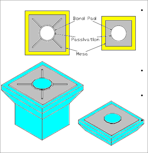
LED Sawing Experiences
|
|
|
Purpose:
- We are able to perform Bevel Cut for special LED dies.
- Require additional breaking process
- Critical in control on un-cut depth (0.5mils) to prevent excessive chipping and double die during breaking
Criticalness Control on Un-cut Depth
- Tape thickness
- Table levelness
- Optimum setup parameter (Z height control)
|
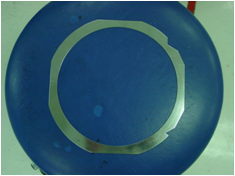
Partial Sawing Experiences
|
|
|
- We are able to perform remount for broken wafer.
- We have SRU (Shape Recognize Unit) to define the shape of broken wafer to reduce the sawing time.
|
| Full Saw |
Partial Saw |
|
Substrate Sawing Experiences
Substrate Component
- Sawing on substrate contain of copper and encapsulant which having different co-efficient expansion.
Critical Criteria
- Copper frame burr and chipping
- Delam on transparent encapsulant
Criticalness Control on Sawing
- Optimum setup parameter (saw speed, define coolant angle, DI water flow rate)
- Chuck table levelness
- Selection of blade type (grit size, concentration range and exposure)
Side Braze Saw Experience
Sawing Concept :
- Engineering wafer to cut a structure out for assembly and testing.
Criticalness Control on Sawing
- Understand saw plan and manually program performing sawing.
Capabilities:
- Wafer thickness: thinnest down to 50 micron (2 mils)
- Saw street: as small as 0.8 mils
Sawing conditions capabilities:
- DI Water resistivity with CO2 bubbler <1M or >10M, RO, H2O2, Triton-X and Diamaflow.
Saw materials capabilities:
- Silicon, GaAs, Silicon Carbide, Copper wafers, Ceramic substrate and PCB.
Wastewater treatment capabilities:
| Capacity |
60 gpm |
| System Treatment |
Treatment Plant rinse water from Plating Bath, Sawing & Scrubber Wafer materials : Silicon, GaAS, InGaN, Silicon Carbite.
|
| Concentrate Areas |
Die and substrate Sawing STM Tin Plate & IDT Lines (Pump < 3,200litres/Month) |
| Operation |
24hrs/day |
Effluent Parameters:
To comply with Malaysian Environment Quality Act 1974 Standard B for the below parameters.
| Parameter |
Unit |
Limit For STD B |
| pH |
|
5.5 - 9.0 |
| BOD |
mg/I |
50 |
| COD |
mg/I |
100 |
| Suspended |
Solids |
100 |
| Tin |
mg/I |
1.0 |
| Lead |
mg/I |
0.5 |
| Nikel |
mg/I |
1.0 |
| Copper |
mg/I |
1.0 |
| Oil & Grease |
mg/I |
10.0 |
|


")